


Embedded Hardware Hacking 101 – The Belkin WeMo Link
Why Embedded Hacking?
Devices that are connected to the Internet or run a full operating system are becoming more and more prevalent in today’s society. From devices for locomotives to wireless light switches, the Internet of Things (IoT) trend is on the rise and here to stay. This has the potential to make our lives much easier; however, the increasing sentience of once analog devices also enables adversaries to target them and potentially misuse them.
With the ubiquity of these Internet-connected devices, there is a surplus of “Things” to exploit. The main intent of this blog post is to generalize how an individual would reverse engineer an embedded device and the process for attempting to find vulnerabilities.
For this demonstration, we will be looking at the WeMo Link, which is a part of the Belkin WeMo LED Lighting Starter Set (http://www.belkin.com/us/p/P-F5Z0489/). There have been vulnerabilities identified in previous iterations of this device; however, these vulnerabilities were more focused on the web services component and not based on analyzing the built-in security of the physical components.
Steps to Analyzing Hardware
There are several steps that an analyst should take when examining their device. These steps, at a high-level, are:
- Research the device
- Identify the components
- Identify debugging ports
- Dump the flash
- Extract/analyze firmware
These steps are crucial to understanding the device being analyzed and are required to help identify vulnerabilities. In the following scenario, I will walk through the aforementioned steps and explain each, the path I took, and what other potential sub-paths one could take, given their specific scenario.
Research the Device
The scope of this project involved examining IoT embedded hardware devices that primarily ran embedded Linux as its operating system. I looked at several IoT devices and decided on the WeMo Link due to its ability to be controlled by a mobile application and to be used for home automation, its utilization of wireless components, and its ability to be controlled over the Internet.
The WeMo product allows a mobile application to dim or turn the bulbs on and off remotely, or add a bit of intelligence to the bulbs by having them sync with the sunrise or sunset automatically. There are two main components that drive the device: the WeMo Link and the WeMo bulb. The WeMo Link is comprised of a WiFi 2.4GHz radio component as well as a ZigBee component that communicates on the same band. In terms of the software, the user downloads a mobile application for their Android or iOS device to initially setup the WeMo Link, which then allows them to control the WeMo bulb.
When initially setup, the WeMo Link broadcasts its SSID of “WeMo.Bridge.XXX”. The user then connects to this AP (Access Point) with their mobile device, shares the user’s wireless AP credentials, and the WeMo takes care of the rest. The WeMo then takes any command sent from the mobile application, sends it to the user’s router, to the WeMo Link, and then transmits the command over ZigBee to execute the command to the appropriate bulb(s). Pretty simple.
Identify the Components
In this example, the brains of the operation appear to be the WeMo Link component. In order to be certain, we need to take the device apart. The lid easily pops off by applying force with a flathead under the lip of the plastic. There are several ways of identifying how to properly disassemble a device – from identifying pull tabs to uncovering screws that are covered with warranty warning tape. In this case, the device had a slightly protruding lid held down by four tabs. Behind the plastic lid were two main components: the mainboard, and the AC/DC converter consisting of a transformer, rectifier, etc.
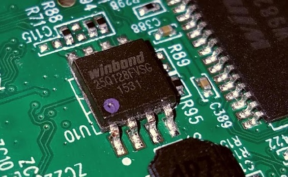
As we examine the mainboard, we will need to identify the datasheets associated with each component in order to get a better idea as to how the device works. On the mainboard itself, what is immediately visible (we will remove the shielding in a bit) is a Winbound W9825G6KH-61 (https://www.winbond.com/resource-files/da00-w9825g6khc1.pdf) 32MB SDRAM and a Winbound 25Q128FVSG (https://www.winbond.com/resource-files/w25q128fv_revhh1_100913_website1.pdf) 16MB serial NOR flash memory with the ability to communicate over SPI (Serial Peripheral Interface) (this will be important later), as seen in Figure 1. The latter chip is used for storing the more permanent memory on the board, even while the device is powered off.
After removing the two metal pieces of shielding on the opposite-side of the board (easily pried-off with a flathead screw driver), we uncover three more main components.
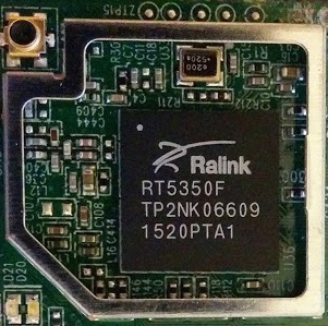
As seen in Figure 2, the first chip is a SoC (System-on-a-Chip) Ralink RT5350F (https://cdn.sparkfun.com/datasheets/Wireless/WiFi/RT5350.pdf), which is a MIPS embedded processor commonly used for networking devices and supports SPI communication, 360 MHz MIPS24KEc CPU core, 802.11n wireless communication, and more. This component is used to drive the device’s main functions, communicate over its debugging interface, interact with its ZigBee component, and communicate with our router over its built-in Wi-Fi component.
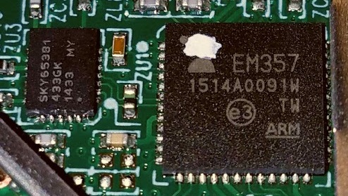
As shown in Figure 3, the other shielded section contains the SoC for the ZigBee device labeled as Silicon Labs EM357 (https://www.silabs.com/Support%20Documents/TechnicalDocs/EM35x.pdf), which handles all of the ZigBee 2.4GHz communication and processing power (32-bit ARM Cortex M3 processor) used to relay information to and from the WeMo light bulbs. The other chip residing in the same section is a SkyWorks SKY65336 (http://www.skyworksinc.com/uploads/documents/200939H.pdf) transmit/receive front-end module used for the ZigBee transmission, which appears to be utilized by the aforementioned Silicon Labs EM357 ZigBee SoC to perform the actual transmission of the data to the light bulbs.
Identify Debugging Ports
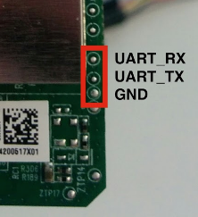
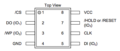
When debugging/interacting with a device, the two most common ways consist of JTAG (Joint Test Action Group) and UART (Universal Asynchronous Receiver/Transmitter). JTAG is a dedicated debugging port implemented as a serial interface used for communicating with the target device. UART is a means of serial communication that can easily be bridged over USB via any UART-to-USB bridge. When looking for UART communication, a lot of times you will see three to four pins that are grouped together with tracings routed to other parts of the board. To help us identify these pins, we can use a multimeter. By touching each of the suspect pins with the positive end on the pad and negative end to a ground (such as the shielding), we can monitor the voltage and identify what the pins are. However, in this case, the WeMo’s circuit board silk screening was friendly enough to label exactly what pads were utilized for interfacing with the device. They were labeled conveniently as UART_RX, UART_TX, GND, and VCC, as seen in Figure 4.
To be sure that the labels are accurate, we can still utilize the multimeter to test each pad’s connection. By powering up the device and monitoring each pin, the UART_RX oscillated throughout a series of voltages. This indicates that data is being streamed across this pad, which is what we will later utilize to view the device’s console. UART_TX is utilized for transmitting commands to the device and can be a bit tricky to identify. This pad also displayed as 3.3V, but given its placement, I did not anticipate this to be VCC. VCC sometimes will also have a thicker trace than the other pads, indicating it is used for supply power. The GND pad provided 0 volts on the multimeter, implying it was the ground pin, and the VCC supplied a steady 3.3 volts, implying it was the power pad. We will utilize these connections later on after we analyze the extracted firmware from the flash dump.
Dump the Flash
As mentioned earlier in the WeMo teardown section of this post, we identified the flash memory that is used to store the bootloader and firmware for this device. This is the core component of the device that an attacker would attempt to modify. We have two ways to dump the memory off of this component, and I will highlight one method. These methods consist of: connecting a test clip to the chip itself while it is still soldered to the board and utilizing a tool such as the bus pirate to dump the flash memory, or desoldering the chip and then placing the chip in a programmer to read the memory off of the chip.
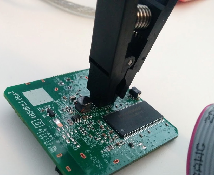
For the sake of being as hardware-oriented as possible, I went with the method of dumping of the SPI flash memory via the bus pirate without desoldering the chip. I wanted to take a non-invasive approach such that my analysis might not be discovered (no physical modifications) by the naked eye. For this method, I purchased a bus pirate from Dangerous Prototypes and an SOIC8/SOP8 test clip (these stand for different types of chip packages, meaning small outlined integrated circuit and small outlined package). This particular flash chip fit perfectly with my 8-pin test clip and was used to make a connection while not removing the chip from the board. I then correctly wired the chip with respect to the bus pirate ports, while following the datasheet and pinout of the chip, as seen in Figure 5.
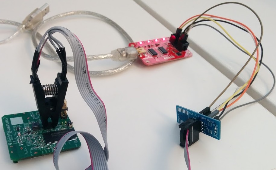
To dump the flash memory from the chip, it must be powered by something. In this case, we utilize the bus pirate’s 3.3v line to provide power to the chip, as seen in Figure 6 and Figure 7.
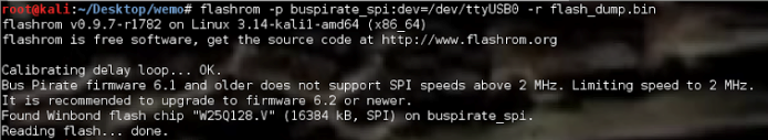
The problem with this is that, at times, voltage injection may occur and wake up other chips on the board. This means that other chips will communicate with our flash chip, interrupting our flash dumping process. This is why it is generally recommended to desolder the chip with a rework station and read the contents of the chip with a programmer. Thankfully, we were lucky and this was not the case. To dump the entire 16777232 bytes (exactly 16MB) worth of content from the flash chip, I utilized a tool called flashrom, which works well with the bus pirate device to extract the flash memory in full, as seen in Figure 8.
Extract/Analyze the Firmware
Now that we have a flash dump from the device, we can use the tool binwalk to analyze the headers within the flash dump to get a better understanding of what the dump consists of, as seen in Figure 9.
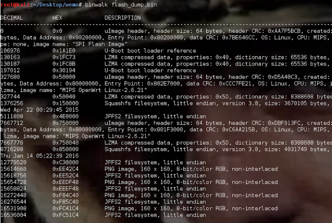
At first glance, we see that the device utilizes U-Boot as its bootloader (common for embedded Linux devices), and that there are several file system types such as SquashFS, JFFS2, and the like. Luckily, binwalk has a very neat feature that can automatically extract as much as it can identify from signatures in the flash dump and provide us with the full filesystem of the device. By running binwalk with the filesystem extraction flag (binwalk -e), we are presented with several filesystems, one of which is displayed in Figure 10.

Within this directory, we can now take off our hardware reverse engineering hat and put on our software reverse engineering hat and begin looking for interesting items such as encryption keys used to sign WeMo device firmware, hashed root passwords, interesting services that may start on boot, etc.
Further Testing
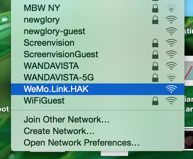
What I found interesting after dumping the flash memory was that all of the memory was directly readable from the chip, and that the bootloader was bundled onto the same flash chip. This implies that, since there are no read controls on the flash chip as well as the bootloader existing on the same (potentially unprotected) chip, I might be able to write my own data to the device. I performed a few tests where I manipulated the flash dump binary itself, such as changing the serial of the device (which in turn changed the wireless broadcasting AP SSID). This initial test was to see if I could successfully modify part of the flash memory to display these changes in a real-world environment, this case being renaming the broadcast AP SSID, “WeMo.Bridge.HAK” as opposed to the original “WeMo.Bridge.CBD”, as seen in Figure 11.
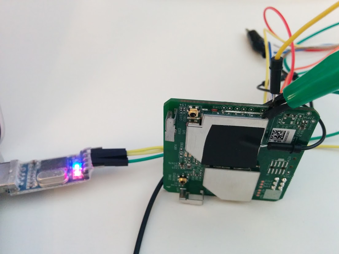
I was encouraged in my efforts because I could write a new binary file to the device, completely overwriting the original content. To examine this further, I needed to make modifications to the flash dump and judge the results by viewing the startup console for the device. This involved connecting to the device’s UART debugging pads, as described earlier, and viewing the output of the console. To interact with the UART_TX pad, I used an alligator clip wrapped with electrical tape to hold down a wire that touched the pad and connected to my UART to USB device, attached to the UART_RX pin. It is important to note that since the device was plugged into an outlet and was already receiving power, that I only needed to connect to the transmission pad(s) as well as ground – but not power. This would have fried the device. As illustrated in Figure 12, I decided to connect the ground wire to the shielding, which already acts as a ground. This was much easier than attempting to connect the ground wire to the corresponding ground pad.
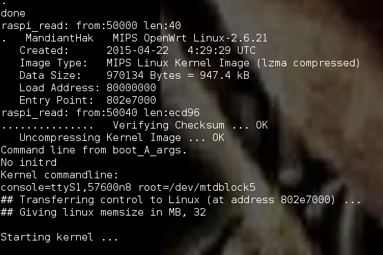
On the software side, I used the program baudrate.py to easily determine the baud rate (transmission rate) of the device via UART. After powering on the device and cycling through several garbled lines of text, I was met with a baud rate of 57600, which presented readable text, displaying the entire boot process of this device, as shown in Figure 13.
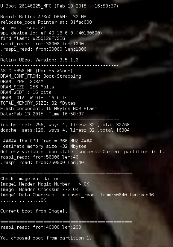
I now had the ability to compare the strings found in the flash dump to what was displayed during the boot process of the device. To confirm my theory of potentially modifying the bootloader, I matched strings found in the binary to what was displayed in the console and attempted to modify those strings and rewrite this section of the bootloader, U-Boot. While using a hex editor to modify the binary file and flashrom to erase/write my file to the flash chip, I successfully modified the strings found in the bootloader process. I changed the bootloader header from “U-Boot 20140225_MFG (Feb 13 2015 - 16:58:37)” to “Mandiant Bootloader (May 18, 2016 – 15:38:25)”, as seen in Figure 14.
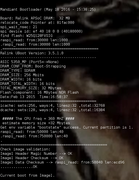
I was also able to modify various field names regarding the image verification process, most likely around the time where the bootloader checks the validity of the firmware, as seen in Figure 15.
The checks present in the image verification process are irrelevant if portions of the bootloader can be modified. In theory, if the above assertions are correct, an adversary could non-invasively rewrite a new, malicious bootloader and firmware to the device, with the ability to perform malicious acts on the user’s network as a trusted device. Such a scenario could consist of a reseller of this product placing a custom bootloader and firmware onto this device, and then selling the product to an unsuspecting customer, having a control point in the user’s network. This could theoretically enable an attacker to intercept traffic on the network, acquire data on the network, modify data, and more.
Remediation
The following recommendations do not take into consideration all of the variables that are involved when making significant changes to a device in order to implement security improvements. These recommendations are things to consider when attempting to remediate the aforementioned scenario.
There are a few hardware-based actions that could be taken that would make it significantly more difficult for an adversary to read/write to the flash chip, among other areas. One such action is to implement hardware authentication chips. This involves storing a cryptographic mechanism on the board along with the required key for decryption, hindering an adversary’s ability to clone or tamper the data on the device. This is a cost-effective method for IoT device manufacturers.
A second action is to protect the bootloader by storing it in protected storage or a SoC, or to require the SoC to communicate with an authentication chip during the boot process. The problem with implementing the bootloader on a flash chip that is unprotected and can be manipulated by disabling the CRC checks in place when decompressing the firmware image on boot and overwriting the image with a malicious one. If the bootloader must be stored on the flash chip, it could be included in OTP (One-Time Programmable) memory, disallowing this area to be written by a third party.
Conclusion
It is important to keep in mind the amount of attention paid to security is generally proportional to the value of the device. Implementing strict security features for a relatively inexpensive home automation system may not make sense for all but the most security-conscious consumer. That said, it is important to understand how easily an adversary can implement a malicious bootloader/firmware with a backdoor, allowing for command-and-control on devices we may rely on in our homes. A device as simple as a wireless light bulb can still be used as an entry point to our home systems.
By taking the previously outlined steps to analyze an embedded device, we successfully identified relevant chips, a UART debugging port, and how to read and write raw data to the accessible flash chip, affecting the boot process of the device. Following the previously defined steps will help you further investigate most embedded devices in order to identify vulnerabilities.
Upon notifying Belkin of our intention to release this research, they provided the following statement:
“Wemo appreciates the work of FireEye and other white hat researchers who often play a critical role in identifying potential security issues and keeping connected devices safe for consumers. As malicious hackers grow more sophisticated, it is critical that we, and other smart home manufacturers, work with these groups to mitigate any serious threats to safety and security.
“Though Wemo is aware of the potential vulnerability published by FireEye in their recent blogpost, we do not believe it is serious enough to warrant what would be a major change to our hardware production. In order to facilitate this attack scenario, a hacker would have to have physical access to a Wemo Link device, tamper with its circuitry and then either return the hacked device or resell it, both of which are extremely unlikely. With this particular vulnerability, there is no remote or even local network threat to users, so we believe that the best way to prevent this is to always purchase new, unopened merchandise from an official Wemo dealer.”
Prepare for 2024's cybersecurity landscape.
Get the Google Cloud Cybersecurity Forecast 2024 report to explore the latest trends on the horizon.