


Shining a Light on SolarCity: Practical Exploitation of the X2e IoT Device (Part One)
In 2019, Mandiant’s Red Team discovered a series of vulnerabilities present within Digi International’s ConnectPort X2e device, which allows for remote code execution as a privileged user. Specifically, Mandiant’s research focused on SolarCity’s (now owned by Tesla) rebranded ConnectPort X2e device, which is used in residential solar installations. Mandiant performs this type of work both for research purposes and in a professional capacity for their global clients.
Mandiant collaborated with Digi International and SolarCity/Tesla to responsibly disclose the results of the research, resulting in the following two CVEs:
- Hardcoded Credentials (CVE-2020-9306, CVSS3.0: 8.8)
- Execution with Unnecessary Privileges (CVE-2020-12878, CVSS3.0: 8.4)
Technical details can be found in Digi International’s 3.2.30.6 software release, and on FireEye’s Vulnerability Disclosures GitHub project (FEYE-2020-0019 and FEYE-2020-0020).
This two-part blog series will discuss our analysis at a high level, explore the novel techniques used to gain initial access to the ConnectPort X2e device, and share the technical details of the vulnerabilities discovered. Topics to be covered will include physical device inspection, debugging interface probing, chip-off techniques, firmware analysis, glitch attacks, and software exploitation.
If you’re interested in continuing the story in Part Two, you can read it now.
FAQ
What devices are affected, and (potentially) how many devices are affected?
The vulnerabilities described in this post affect ConnectPort X2e devices as well as the SolarCity rebranded variant. Other vendor devices may also be vulnerable. It is unclear how many ConnectPort X2e devices are deployed in the wild.
How is the issue being addressed?
Mandiant worked independently with Digi International and Tesla to remediate the vulnerabilities. Mandiant would like to thank Digi International and Tesla for their cooperation and dedication to improving the security of their products.
How would an attacker exploit these vulnerabilities?
An attacker with local network access (such as being connected to an individual’s home network via Ethernet) to a vulnerable X2e device can exploit CVE-2020-9306 and CVE-2020-12878 to gain privileged access to the device.
Who discovered these vulnerabilities?
Jake Valletta (@jake_valletta), Sam Sabetan (@samsabetan)
Technical Analysis
Device Overview
Before diving into the details, we’ll discuss the ConnectPort X2e device (referred to as X2e device throughout the post) at a high level. The X2e device is a programmable gateway that connects to and collects data from ZigBee devices. It is commonly used as a Smart Energy gateway to interpret and send energy readings from a residential Solar Inverter. Vendors will often purchase an X2e device and configure it to read power consumption generated by a customer’s Solar Inverter. Figure 1 outlines a typical residential solar installation and highlights the X2e’s role.
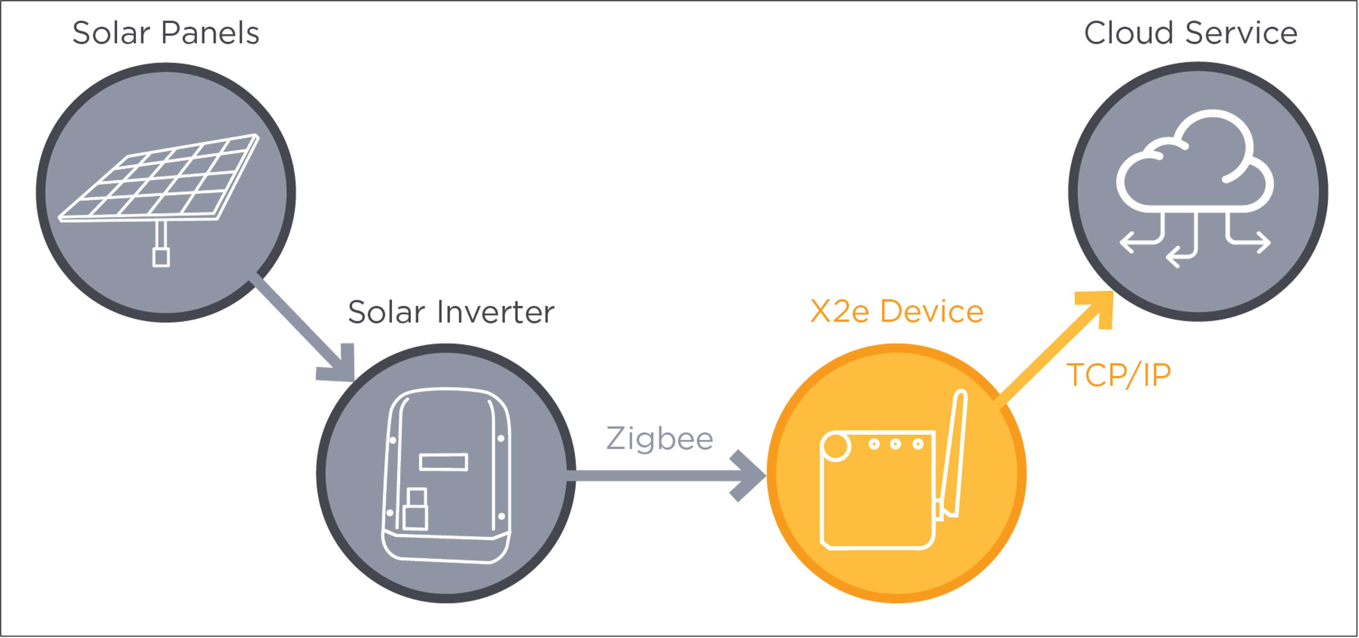
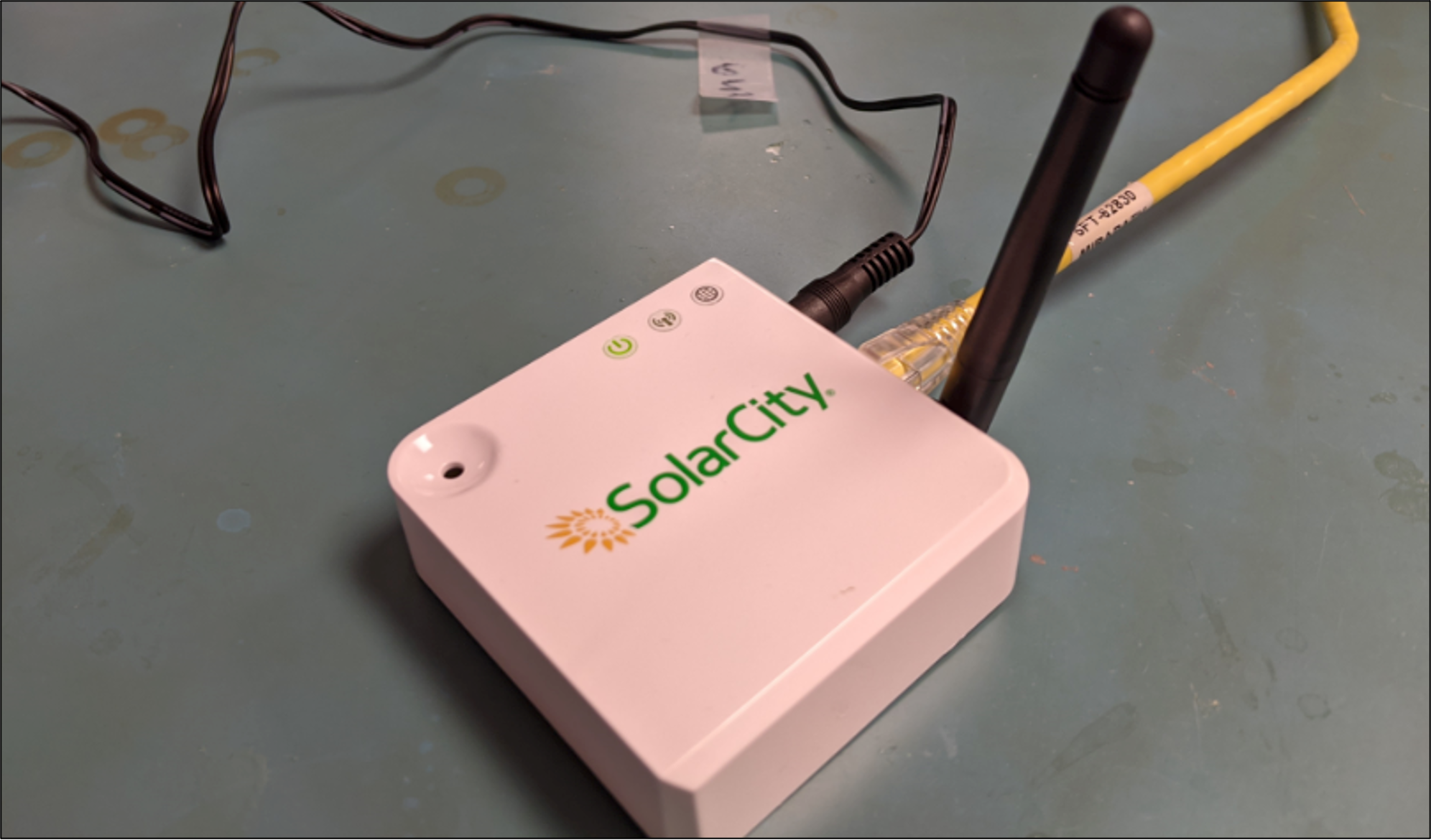
For our research, we focused on the X2e device used by SolarCity, now Tesla, to retrieve data from residential solar installations. A typical setup would involve SolarCity providing a customer with a gateway that would be connected to the Internet via an Ethernet cable on the customer’s home network. Figure 2 shows one of the SolarCity branded X2e devices that we tested.
Without even plugging in the X2e device, we know of at least two separate interfaces to explore: the Ethernet interface and the ZigBee radio. Note that we did not review the ZigBee interface between the X2e and a solar invertor, and that interface will not be covered in either Part One or Part Two of this series.
Initial Analysis and Physical Inspection
Network Reconnaissance
We started our research by assessing the X2e device from a network perspective. By using nmap, we discovered that the device exposed both SSH and HTTP/HTTPS, shown in Figure 3.
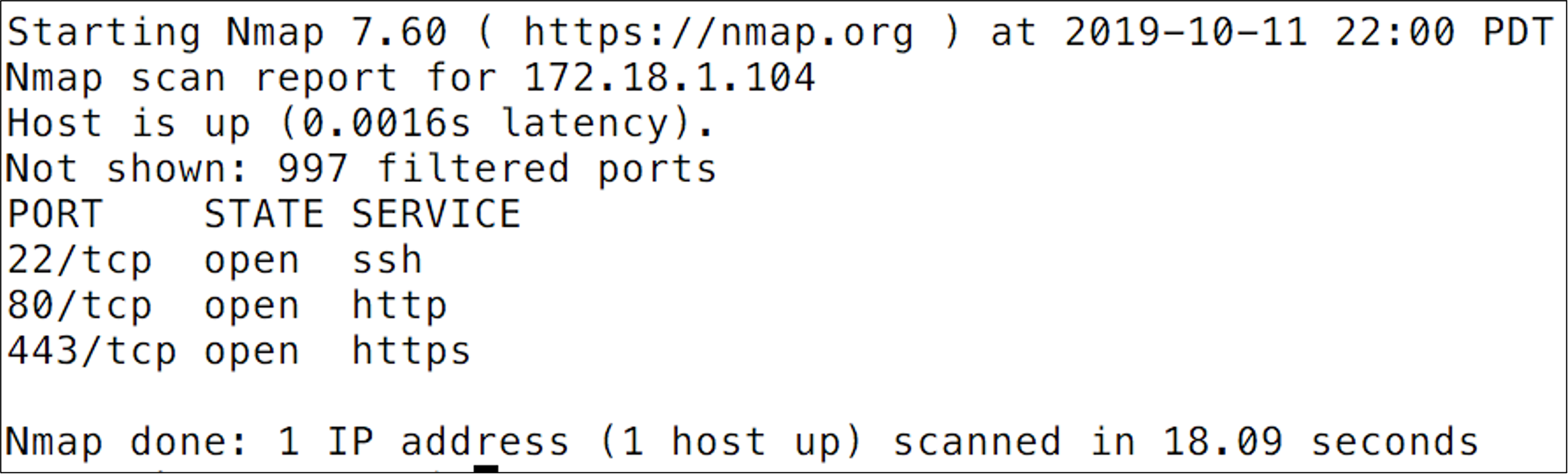
Upon accessing these services remotely, we noted that both services required authentication. We also performed limited brute force attempts, which were unsuccessful. Additionally, the underlying services were not vulnerable to any public exploits. With not many network-based leads to follow, we shifted our analysis to a hardware perspective to determine if any local attacks may be possible to gain initial access onto the device.
Physical Board Inspection
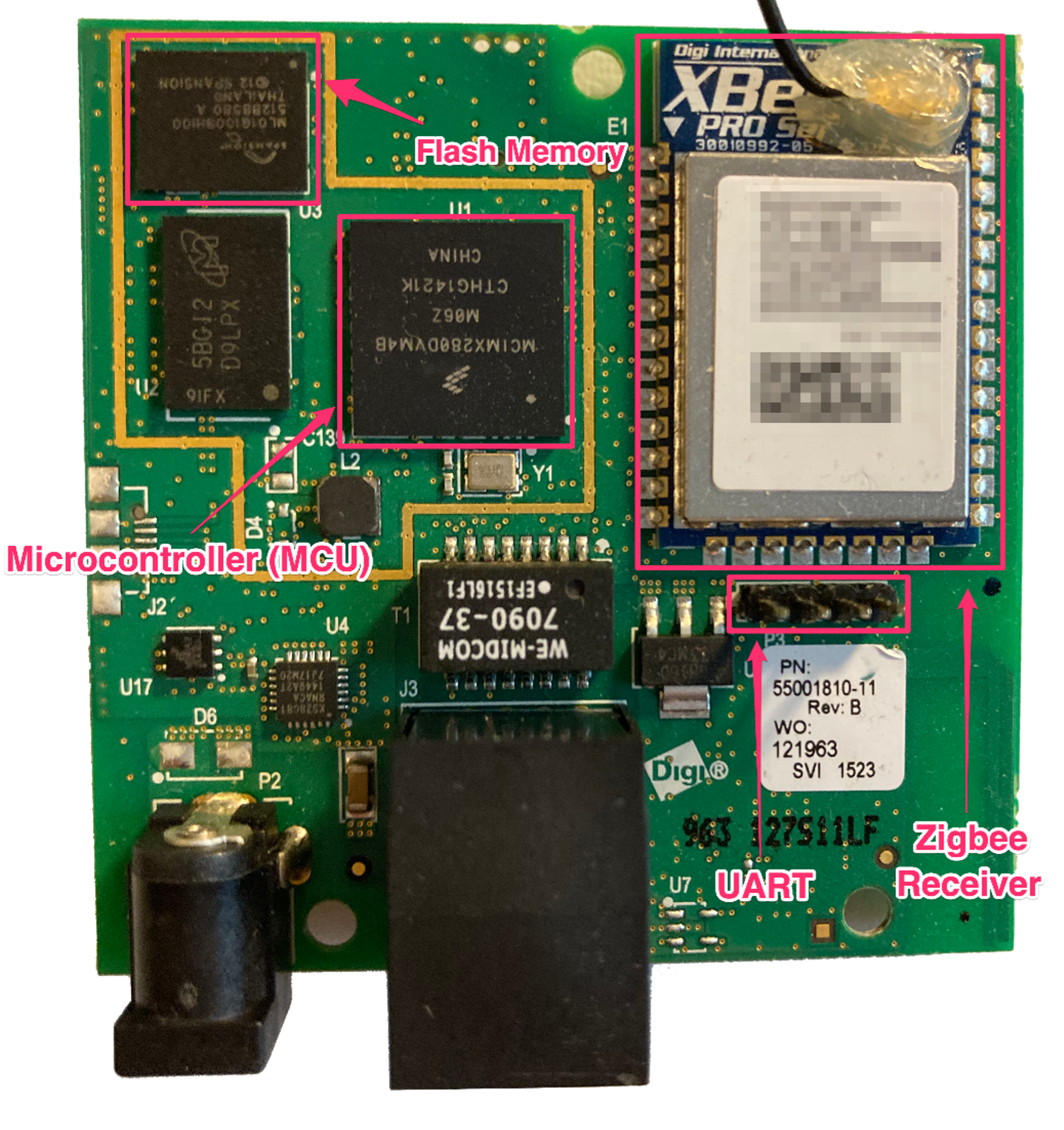
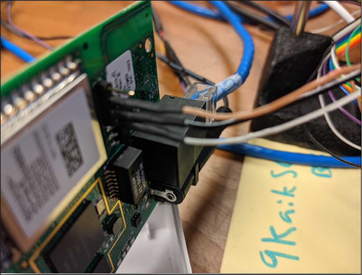
To begin our hardware analysis, we removed the plastic casing from the device and mapped out the various integrated circuit (IC) components and searched for potential debugging interfaces. Inventorying the components present on the circuit board (also known as a PCB) is a crucial step in understanding how the device was designed and what can be expected down the road. Figure 4 shows the mapped-out components as well as a cluster of pins that resembled a typical 3-pin universal asynchronous transmit/receive (UART) connection, a common debugging interface on embedded devices.
Without a remote connection to the X2e device, UART is an attractive target. UART typically provides the equivalent functionality of a service like SSH or Telnet and the added benefit of watching verbose output during system boot. To determine if the cluster of pins was a UART interface, we first soldered a 3-pin through-hole header to the PCB. Using a combination of continuity tests with a multimeter and the digital logic analyzer Saleae, it became apparent that we were in fact dealing with a UART interface. The Figure 5 shows the three pins (Ground, TX, RX) connected to the header. Attached to the other end of the three wires was a FTDI serial TTL-232 to USB adapter, which was connected to a Linux virtual machine.
In addition to correctly identifying the UART pins and a UART to USB adapter, we also needed software to read/write from the interface as well as knowledge of the baud rate. Baud rates vary but typically follow standard values, including 9600, 14400, 19200, 38400, 57600, and 115200. Using the python module pySerial, we connected to the USB adapter and tried standard baud rates until one of the rates produced readable ASCII output (an incorrect baud rate will typically produce non-readable output), and determined the X2e used a baud rate of 115200.
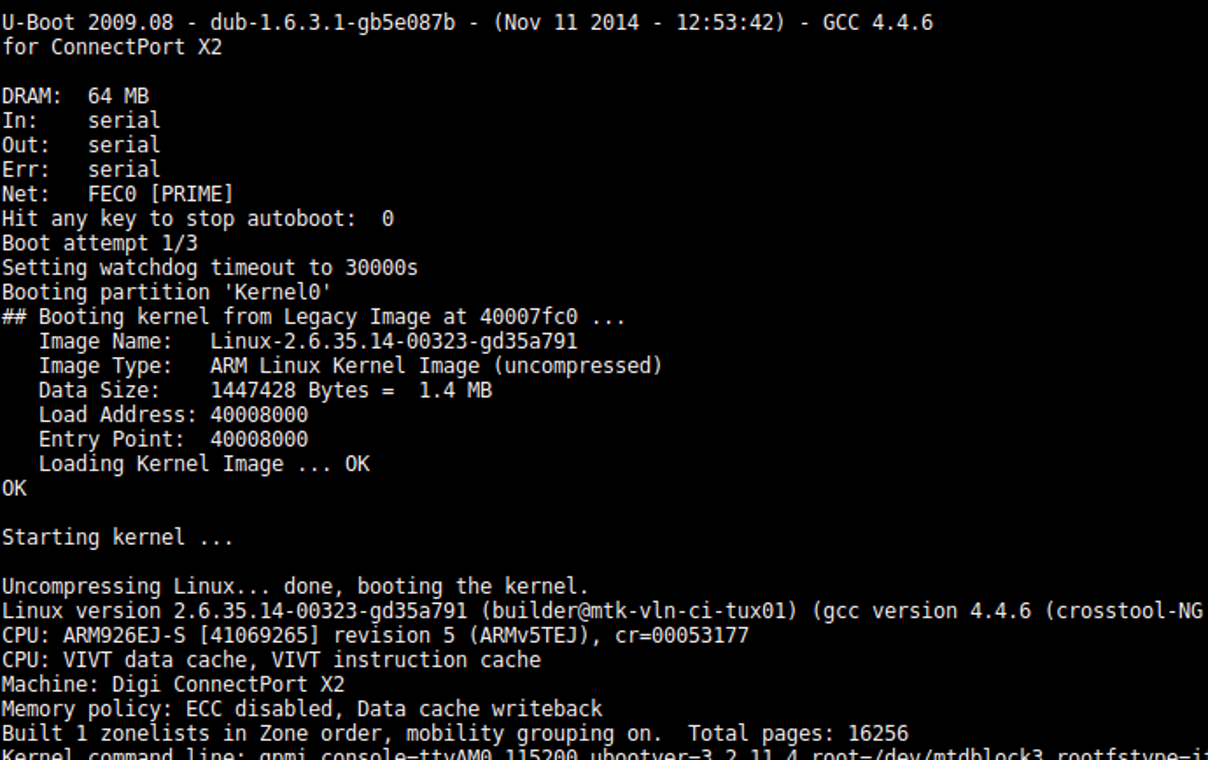
Upon booting the X2e, we noted output from the BootROM, bootloader (which was Das U-Boot 2009.8, a common embedded bootloader), as well as output from the Linux kernel transmitted over the UART connection, shown in Figure 6.
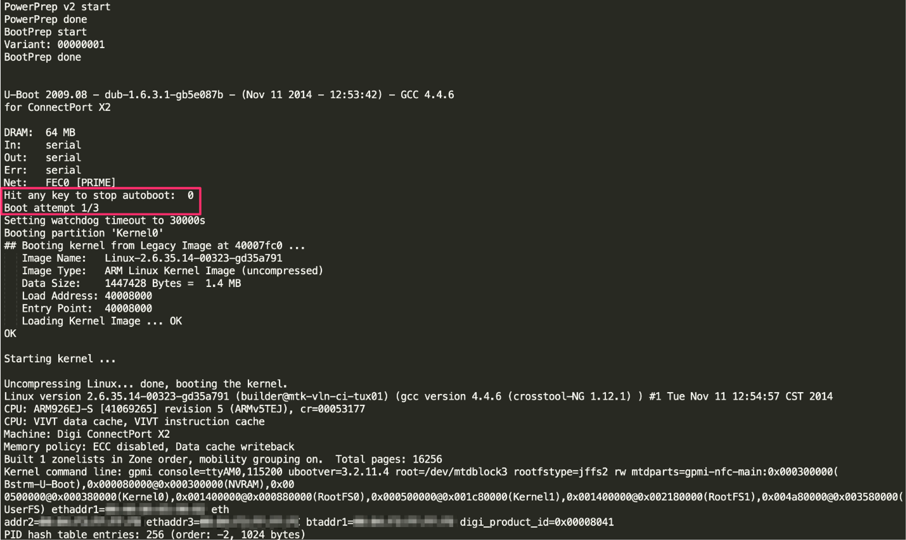
Many configurations of U-Boot allow a physically connected user (using an interface such as UART) the ability to interrupt the boot process; however, this configuration explicitly disabled that feature, shown in Figure 7.
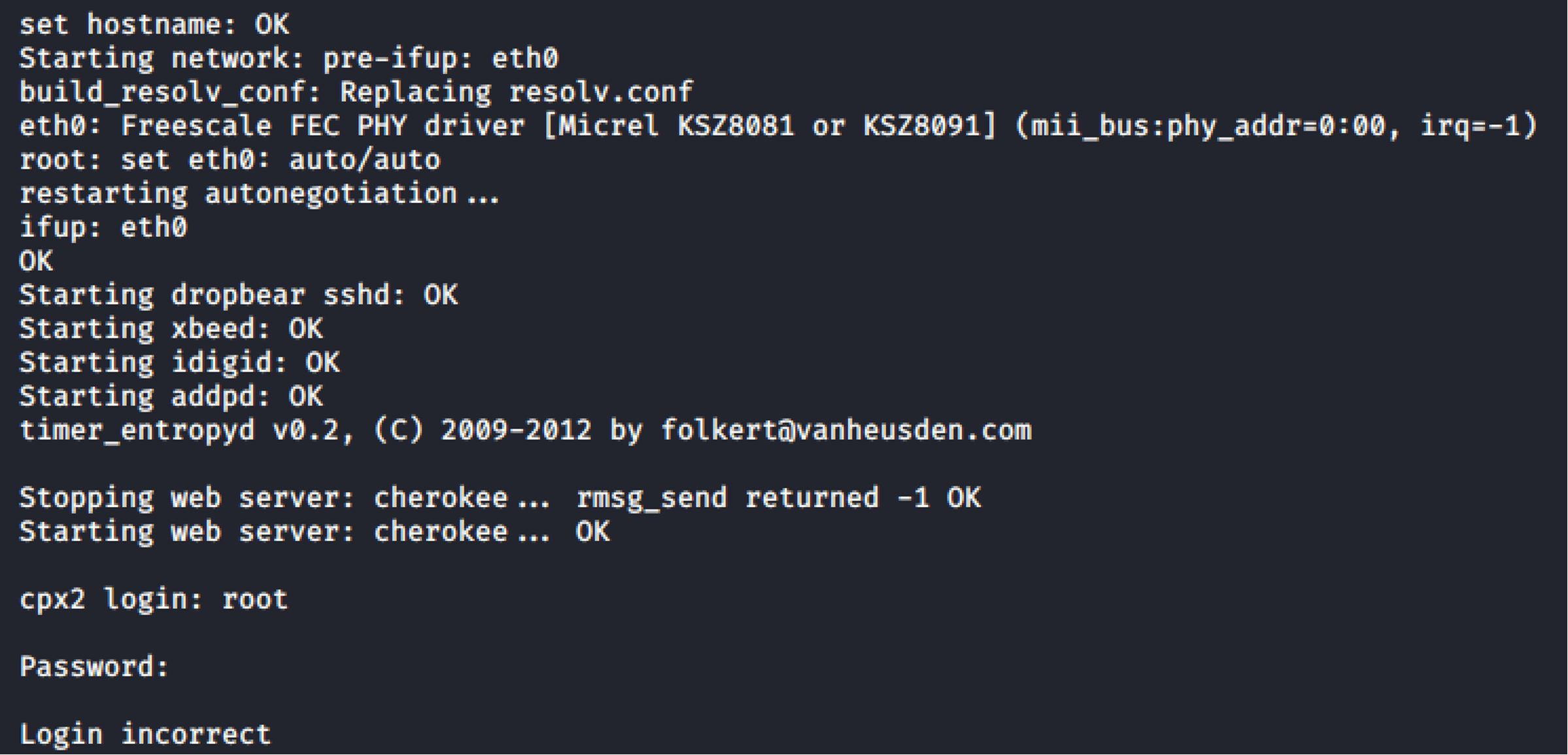
Interrupting a bootloader is attractive to an attacker, as often the boot parameters passed to the Linux operating system can be manipulated to control how it will load, such as booting into single user mode (typically a recover shell) or mounting filesystems as read-write. In the case of the X2e, the UART connection was mapped to a Linux TTY which required username and password authentication, shown in Figure 8.
Without any ability to interrupt the boot process or credentials to authenticate to the X2e, we were faced with another dead end. We then shifted our analysis to obtaining the firmware stored on the X2e’s non-volatile storage.
Chip Removal and Data Extraction
In this section, we’ll cover the basics of non-volatile memory, often referred to as “flash memory”, present on embedded devices as well as the process used to extract content from the chip. As mentioned, taking inventory of the components on the PCB is an important first step. Figure 9 shows the suspected flash chip present on the PCB magnified under a digital microscope.
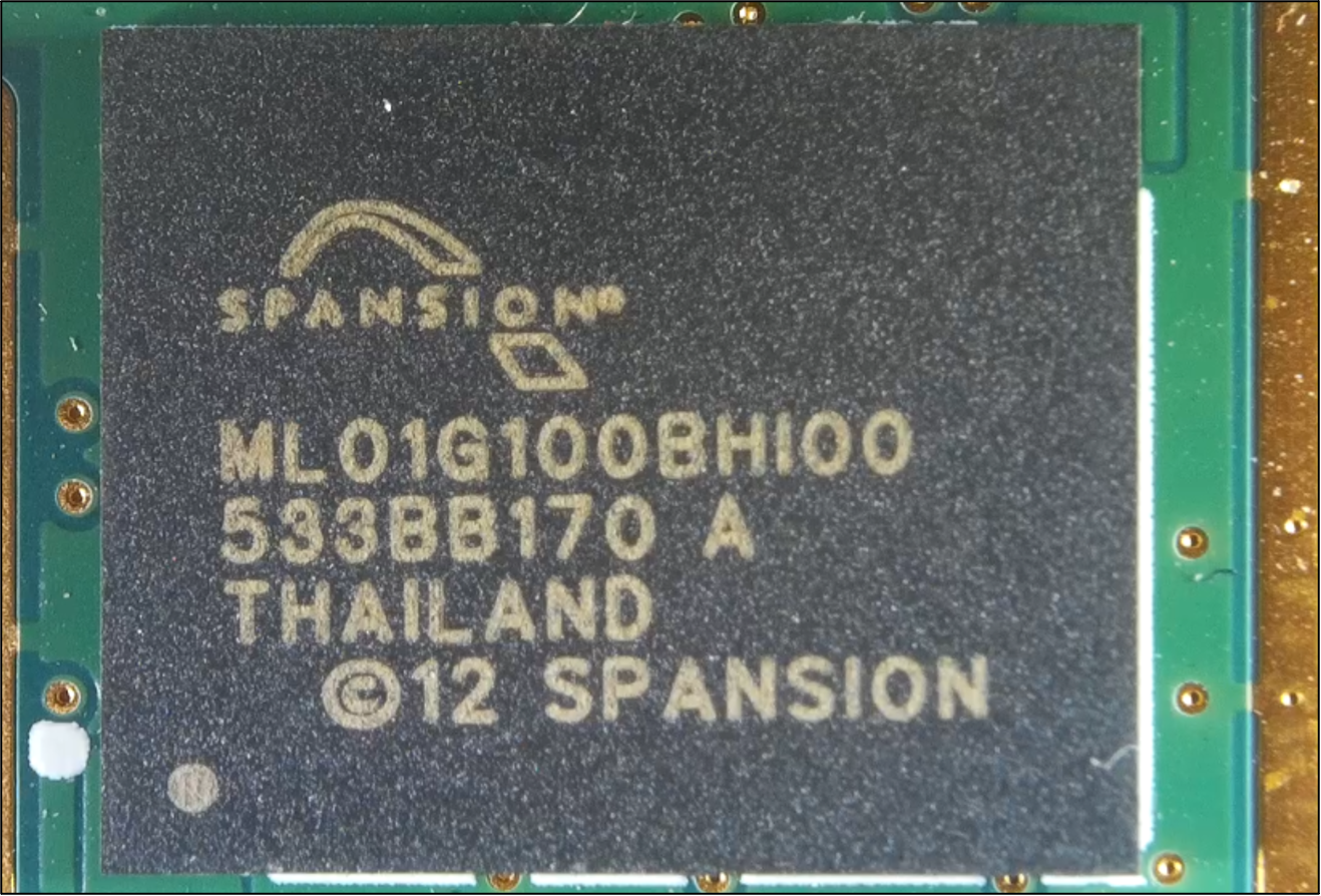
The visible markings seen in Figure 9 are important as they allow us to determine the manufacturer and model of the flash, which will assist us with obtaining the datasheet for the chip. In our case, the NAND we were dealing with was a Spansion S34ML01G1.
NAND Overview
Before we talk about acquiring the firmware from the NAND chip, it’s important to first understand the various scenarios that embedded devices typically follow.
NAND verses NOR: These fundamentally different technologies each have their own benefits and drawbacks. NAND is cheap but suffers from high probability of “bad blocks,” or areas that are corrupt sometimes directly from the factory. As such, protections and considerations need to be present to be able to protect against this. NAND is also much faster to erase and write, making it ideal for storing file systems, kernels, and other pieces of code that may need to be reset or changed. NOR has significantly faster read times but is not as flexible with accessing data and has low erase and write speeds. NOR is usually used for low-level bootloaders, hardcoded firmware blobs, and other areas that are not expected to change frequently. The X2e uses a NAND flash.
Serial verses Parallel: This refers to how the data is accessed and is typically visually identifiable. If there are a large number of pins, the flash is likely parallel. Serial NOR chips can be small in size and typically need eight or fewer pins to function. Common serial interfaces are Serial Peripheral Interface (SPI) or Inter-Integrated Circuit (I2C), while a common parallel interface for NAND is Open NAND Flash Interface (ONFI2.0, ONFI3.0). The X2e is a parallel flash.
IC Form Factor: Another visually identifiable trait—form factor (or “package”)—refers to how the chip is attached to the PCB. There is a long list of options, but common surface-mount flash packages include small outline package (SOP), thin outline small package (TOSP), or a variant of ball grid array (*BGA). The key distinction here is SOP and TOSP expose the pins, while BGA conceals the pins under the package. The X2e is BGA63, also referred to as a 63-pin BGA package.
Managed verses Unmanaged Flash: This one is more applicable to NAND, for reasons alluded to in the NAND verses NOR section. As stated, NAND needs help to manage the integrity of the data. With unmanaged NAND, the IC reserves sections of the flash (often called “spare” area) for someone else to manage the data. This is typically implemented as either a kernel driver or an external NAND controller. Managed NAND means that the IC package includes the controller and transparently manages the data. This is extremely common in embedded devices, as either embedded MMC (eMMC) or universal flash storage (UFS). The X2e uses unmanaged flash and is controlled by the main microcontroller present on the PCB.
With the basics out of the way, we proceeded with physically removing the chip from the PCB.
Chip Removal
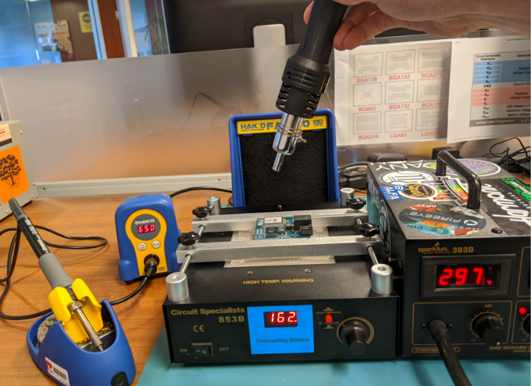
Physical chip removal is considered a destructive approach but can certainly be performed without damaging the PCB or the flash chip itself. When presented with removal of BGA packages, the two most common removal techniques are either hot air or infrared light (IR). Commercial solutions exist for both hot air and IR, but cheaper options exist with hot air removal. We opted to use hot air on the X2e.
To minimize damage to the PCB and flash, a PCB heater or oven can be used to slowly bring the entire PCB to a temperature right below the solder melting point. This will reduce the amount of time we need to focus our hot air directly onto the flash IC and help with reducing the heat dissipation into the PCB throughout the process.
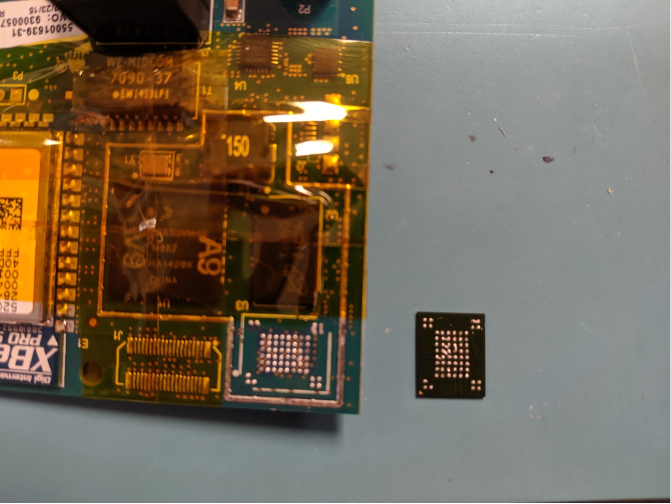
One final trick that can be used to minimize nearby chips from being damaged or lost (due to the air pressure) is the use of high-heat resistant tape, commonly referred to as Kapton tape. Figure 10 shows the PCB wrapped in Kapton tape to protect nearby components.
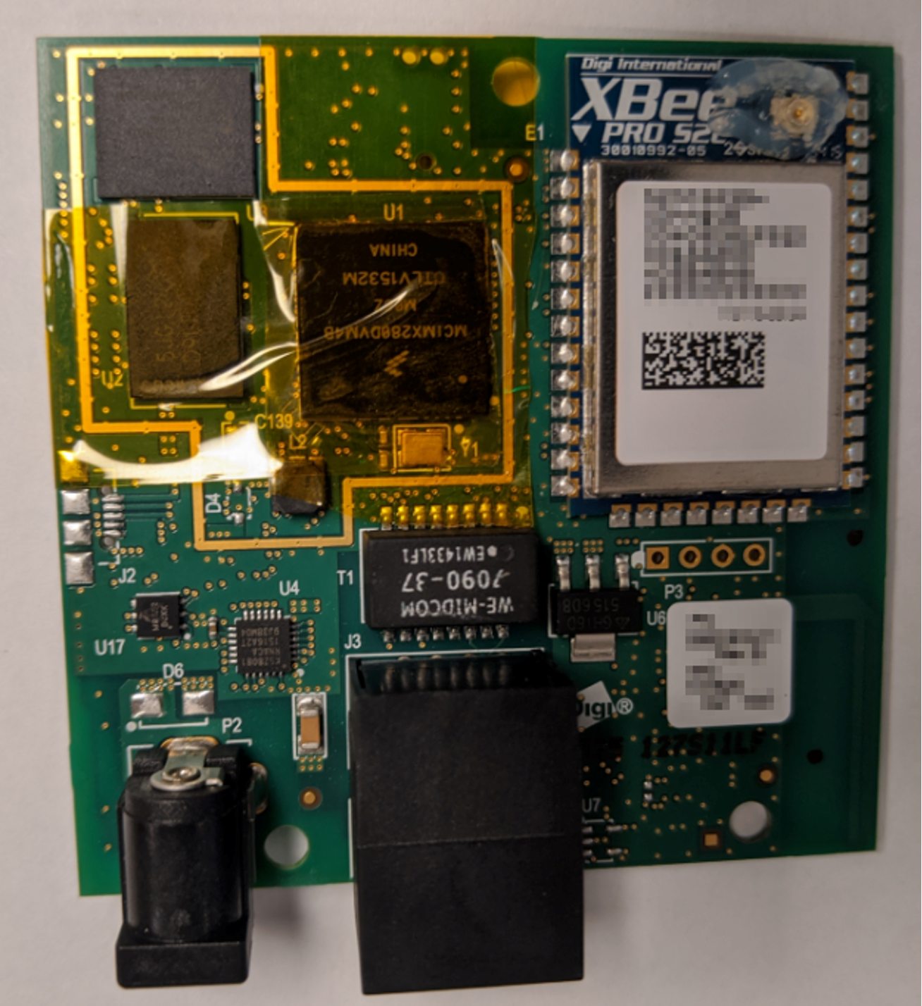
Figure 11 shows an example setup with the X2e PCB inserted into a PCB heater, with a hot air gun suspended over the IC.
While using the hot air to warm the IC and surrounding areas, we gently nudged the flash to see if the solder had become molten. Once the chip appeared to be floating, we quickly removed the chip and let it cool for about 30 seconds. Figure 12 shows the IC flash removed from the PCB, with the solder still present on the BGA pads.
Before inserting the NAND into a clam-shell chip reader, the leftover solder must be removed from the flash. This can be accomplished using a soldering iron, high-quality flux, and de-soldering wick. Once removed, isopropyl alcohol and a toothbrush are highly effective at removing the leftover flux residue and cleaning the chip.
In the next section, we’ll attempt to extract the data from the NAND chip using a multi-purpose chip programmer.
Data Extraction
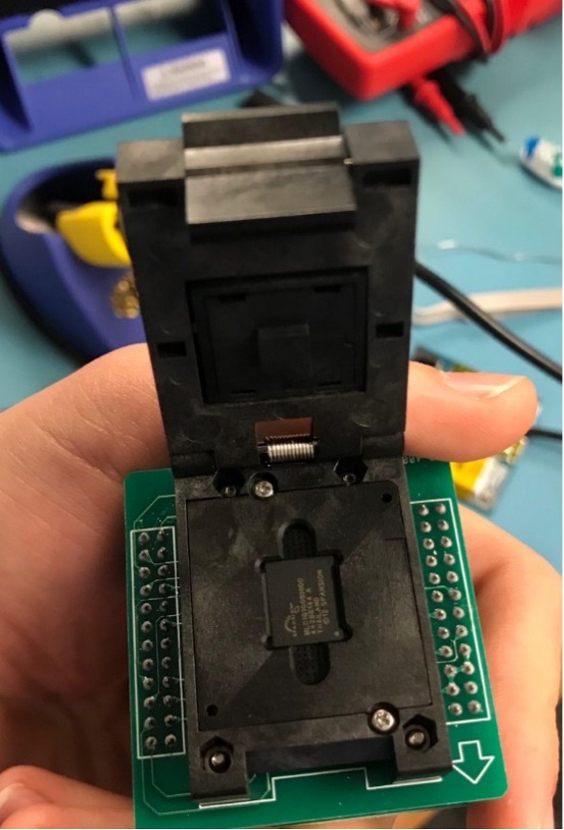
With the cleaned flash chip in hand, we can now explore options for reading the raw contents. Commercial forensic acquisition devices exist, but a quick eBay or AliExpress search will produce a multitude of generic chip readers. One such device, the XGecu Pro, supports a variety of adapters and chipsets and connects to a Windows machine using USB. It also comes with software to interface with the XGecu Pro and can even auto-detect flash. To connect the Spansion NAND to the XGecu Pro, we also purchased a clamshell BGA63 adapter. Figure 13 shows the NAND inserted into the clamshell reader, and Figure 14 shows the clamshell adapter connected to the XGecu Pro device.
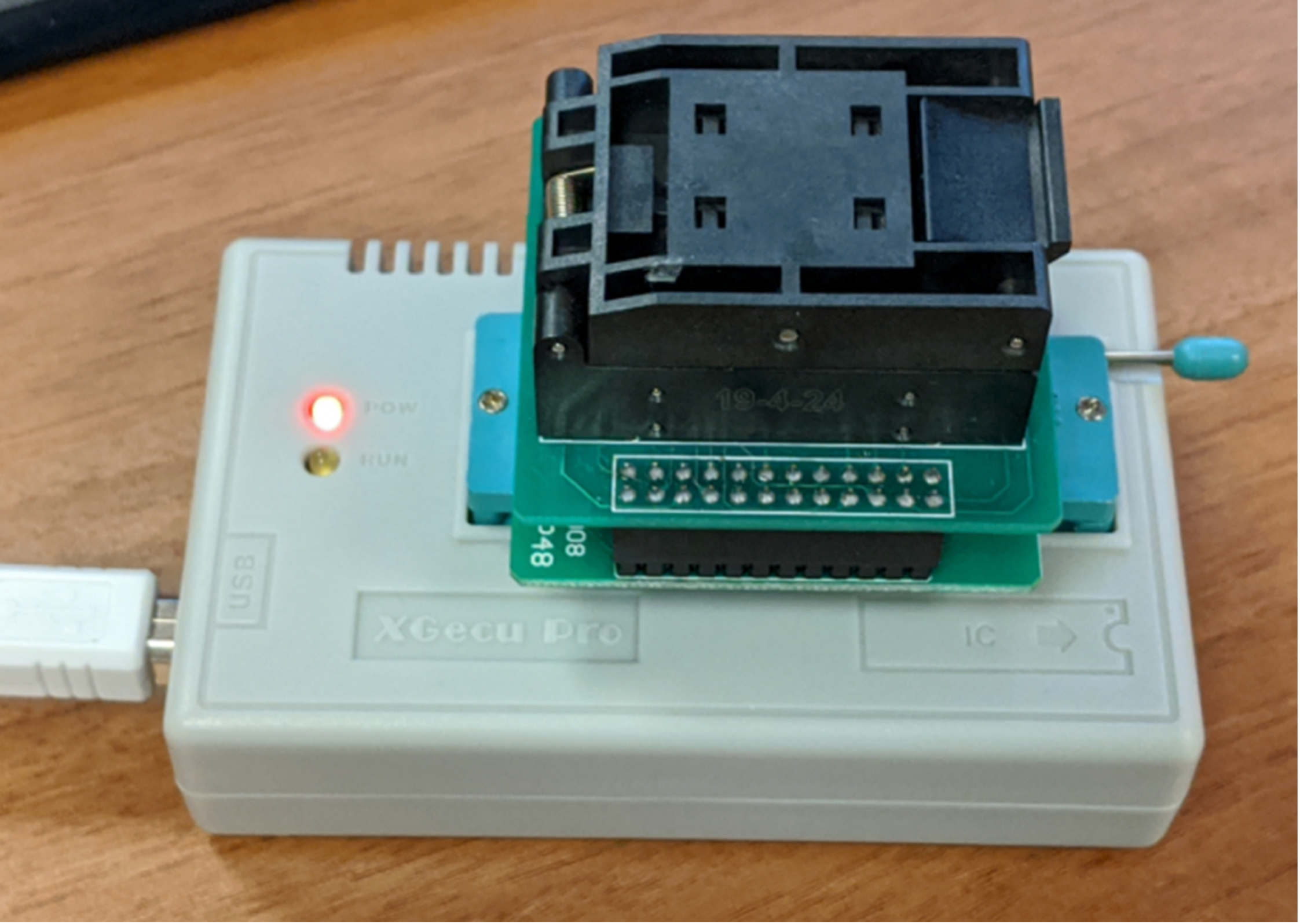
Using the XGecu Pro software, we can read the entire contents of the flash to a binary file for further analysis. Since these are not commercial solutions, it is a good idea to perform two or three reads and then diff the extraction to confirm the content was read without errors.
Firmware Analysis
Cleaning and Mounting
With our fresh NAND dump in hand, the next step was to parse out any relevant firmware blobs, configurations, or filesystems. The go-to tool for starting this process is binwalk. binwalk does a fantastic job of detecting filesystems, bootloaders, and kernels. In addition, binwalk can calculate entropy (detecting packed or encrypted data) and identify assembly opcodes. Figure 15 shows partial output of running binwalk against the NAND dump.
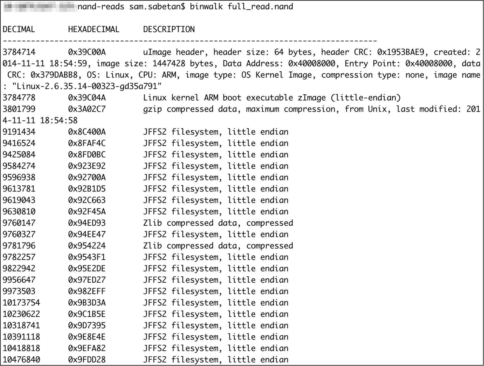
We can see from the output that binwalk successfully identified what it believes are U-Boot uImage headers, Linux kernel images, and more than a dozen Journaling Flash File System version 2 (JFFS2) filesystems. JFFS2 is a common filesystem used in embedded devices; Unsorted Block Image File System (UBIFS) and SquashFS would also be common.
At first glance, the output appears to be promising; however, it is highly unlikely that there are actually that many JFFS2 filesystems present on our NAND. Another indication that something isn’t quite right are the hexadecimal offsets – they don’t appear to be clean, uniform offsets. It is far more common that the offsets of the items identified by binwalk would align with NAND page offsets, which are a multiple of 2048.
In order to understand what is occurring here, we need to revisit a characteristic of unmanaged (or “raw”) NAND ICs described in the NAND Overview section. To recap, raw NAND requires additional bytes per page for use by higher-level components to attest to the validity of the page, typically implemented as a defined “bad block” marker and a per-page (or subpage) Error-Correcting Code (ECC). Without going too deep into ECC fundamentals, ECC provides the ability for higher-level processes to detect n number of bad bits on a page and to correct m number of bits.
Since our goal here is not to perform forensics on the raw NAND, our immediate objective is to remove any ECC bytes or other non-data related bytes from the NAND dump. The MCU is ultimately the system manipulating the raw NAND, so understanding how our MCU, which was an NXP iMX28 series MCU, manages NAND is critical to being able to perform this.
Fortunately for us, this process has already been explored by the security community, and iMX parsing libraries exist to manipulate the raw NAND dump and remove existing extraneous data. Figure 16 shows the results of re-running binwalk on the output of the imx-nand-convert script.
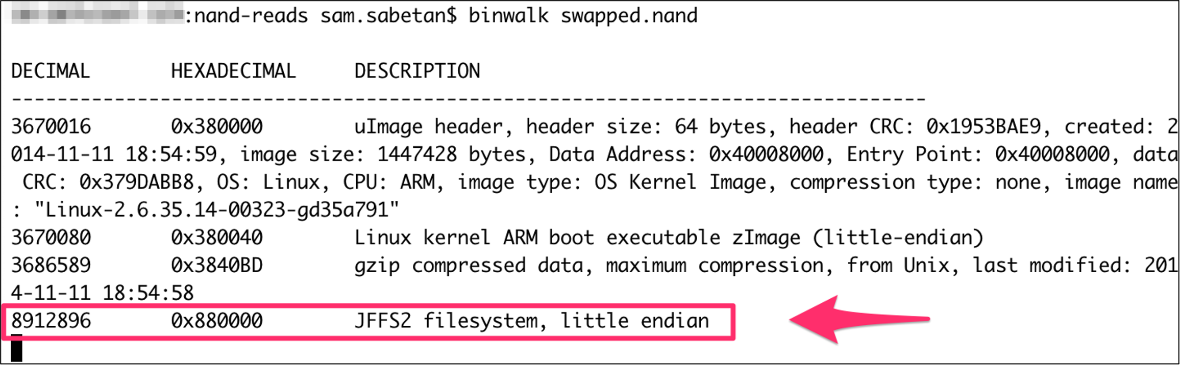
This time, we see only one JFFS2 filesystem, at the very round offset of 0x880000. Using the extraction (-e) feature of binwalk, we can now obtain parsed versions of the U-Boot bootloader, Linux kernel, and JFFS2 system.
The final hurdle we need to overcome is mounting the extracted JFFS2 filesystem in a way that allows us to explore the contents. On Linux, the easiest way to perform this is to use the mtd, mtdblock, and nandsim kernel modules. The nandsim module simulates a given NAND device and uses the mtd and JFFS2 subsystems to parse and manage appropriately. The key piece of information that needs to be passed to the nandsim module is the ONFI chip identifier, which can be obtained from the NAND datasheet or by requesting the ID from the IC using a generic reader (like the XGecu Pro used in the Data Extraction section). A list of supported IDs is also provided by the mtd maintainers. Getting the parameters correct is a bit of luck and magic and may require you to compile your own version of the nandsim module; that process will not be covered in this post.
Figure 17 shows the steps required to simulate the correct Spansion NAND and mount the JFFS2 filesystem in the form of a Makefile target.
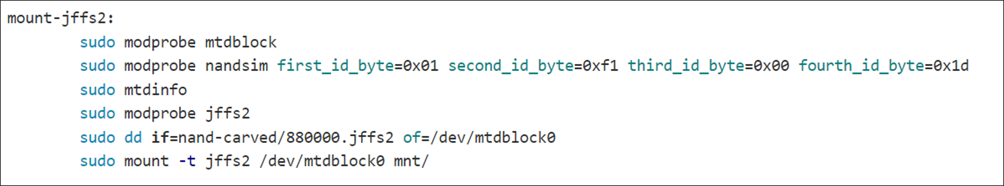
By running make mount-jffs2, we can quickly prep and mount the JFFS2 filesystem and explore the contents as we would any filesystem.
Accessing the Filesystem
In the last section of this post, we’ll walk through our analysis of the JFFS2 filesystem. Remember that our end goal is to obtain a remotely exploitable bug that will permit privileged code execution. With that in mind, some areas of interest are running daemons/processes, system startup logic, and credentials for services listening on the network. The first stop was reviewing the /etc/shadow file to see if there were password hashes for the root user as well as other system users. A quick check of this file determined there was no password hash for the root user, which indicated we would not be able to authenticate using password authentication. We noticed that two other password hashes were present, for the addpd and python users, shown in Figure 18.
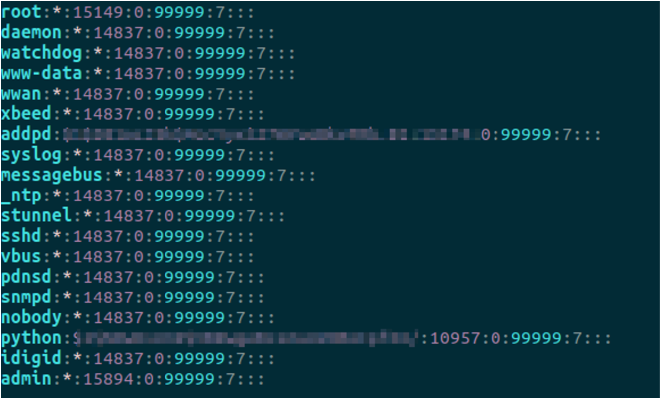
The addpd user had a weak default password but was unable to authenticate using remote methods, and we were ultimately unable to crack the python user’s hash using internal GPU-based servers.
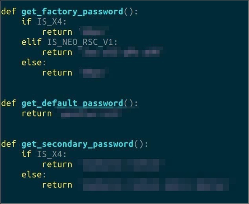
Additionally, we were interested in processes that are launched during system boot or post-boot. The directory /WEB/python/ contained a ZIP archive called _x2e.zip, which contained over 200 compiled Python scripts (PYC files), which were loaded on system boot. Using the decompiler uncompyle2, we unpacked these files for review. One file that stood out by name was password_manager.pyc, a file used to reset the login password upon successful boot-up. The file contained five hardcoded and plaintext credentials that mapped to the python system user. These credentials could be used to access the web interface and SSH, shown in Figure 19. Mandiant confirmed different passwords were used for different versions and connectivity states. Mandiant reported this to SolarCity and was assigned the CVE number CVE-2020-9306.
With the correct password, we were finally able to connect to the web and SSH ports on a running X2e, but unfortunately only as the less-privileged python system user. While this was a great start, it didn’t satisfy our final objective, which was to remotely compromise the X2e as a privileged user. In Part Two of this blog series, we will explore additional avenues to further compromise the X2e.
Conclusion
In Part One of this two-part blog series, we covered an overview of the X2e, our initial network-based reconnaissance, PCB inspection techniques, physical debugging interface probing, chip-off techniques, and firmware analysis. Using these methodologies, we were successfully able to remotely compromise the X2e device as a non-administrative user due to hardcoded credentials (CVE-2020-9306). In Part Two, we will re-investigate physical attacks against the X2e in the form of glitch attacks, re-explore the U-Boot bootloader, and finally demonstrate an attack to remotely compromise the X2e device as a privileged user.
To continue reading, check out Part Two now.
Prepare for 2024's cybersecurity landscape.
Get the Google Cloud Cybersecurity Forecast 2024 report to explore the latest trends on the horizon.